Apr 04

This is part 2 of my hacking adventures on the HT-A1. To see part 1, click here

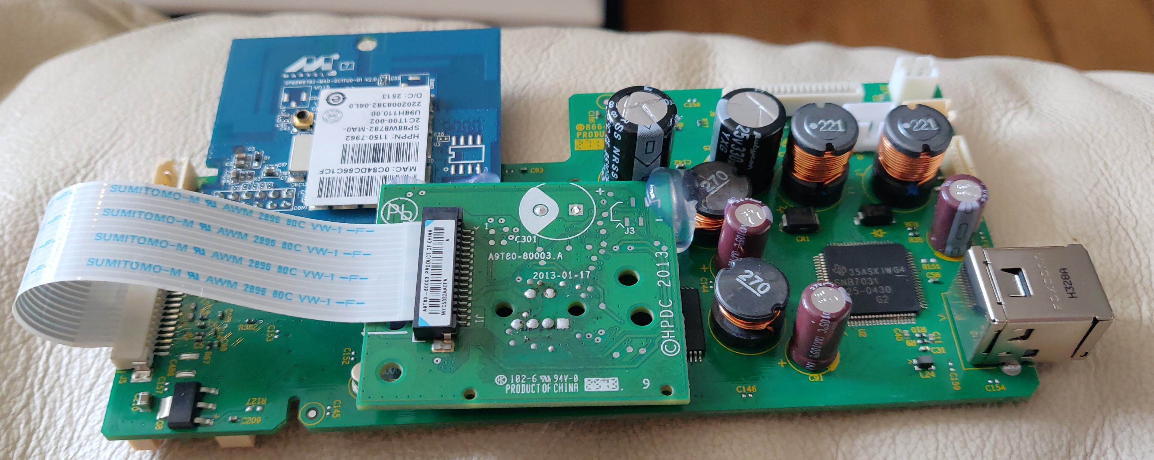
Mounting the USB-hub and WiFi-module never came to be (i lost interest and figured it would be hard to add the missing features in software since i’m no expert at embedded linux and i don’t have the sources for the software the camera is running.

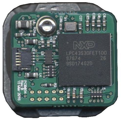
Browsing the internet it became apparent that Seek is now officially stating that they sell OEM modules and you can buy a development kit with SDK etc. I had a look at their pictures and it was clear that the module that the HT-A1 is using a variant of their “Mosaic” thermal core.

Now, what happens if i load the Seek app and connect this to my smartphone? Will the app recognise the module?

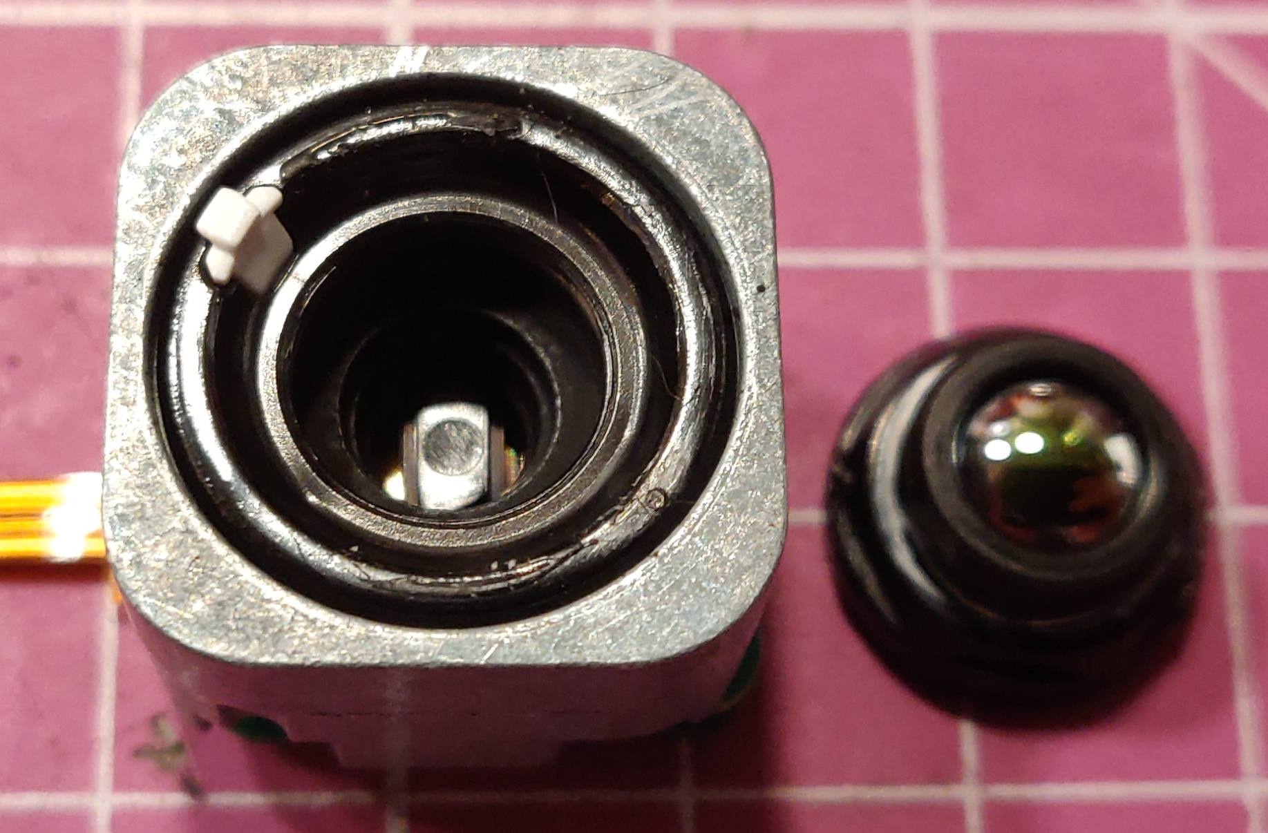
Well only one way to find out i think. I found a suitable piece of flat flex cable that handily went from the 0.5mm pitch to 1mm pitch (so soldering would be a tad easier) I cut it to size so it would fit the small 5 pin connector on the Mosaic core. The docs from Seek says that the Mosaic core is good from 3.3 to 5.5V. I didn’t immediately saw any reasonably sized voltage regulator on the module from the HT-A1 so instead of taking any chances i put two standard 1N4007 diodes in series with VCC to drop the voltage to 3.6V.

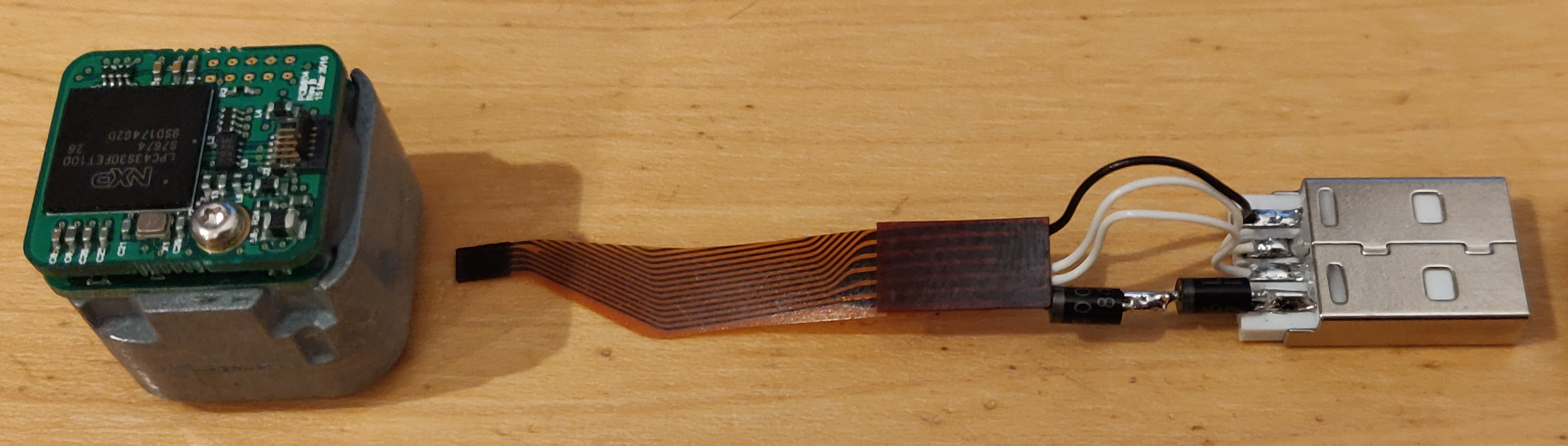
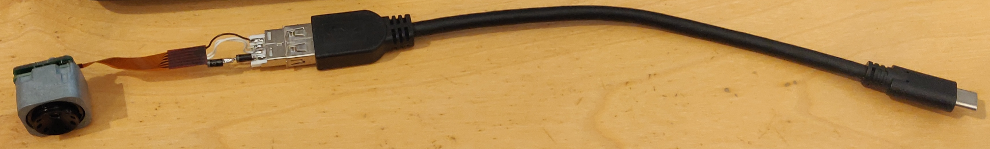
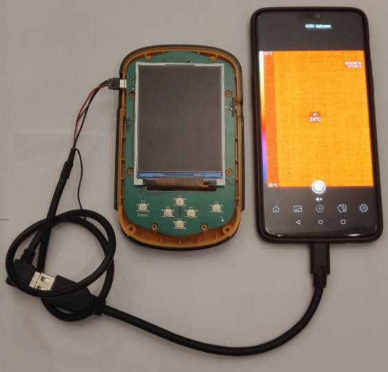
I made a concoction of this custom cable and an USB-C OTG cable that would plug into my Oneplus 6-phone.

I went into settings on Android and turned on OTG support so the port would supply power, plugged in the cable and was met with a friendly popup asking if i would allow Seek Thermal to access PIR206 Thermal Camera? – Hell yes!

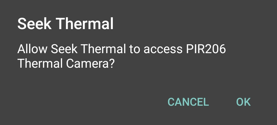
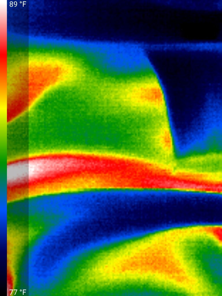
Pressing OK, nothing more happened. I opened up the Seek app and in the top it said “Unknown” as connected. Pressing the name opened up the preview – it works 😀

OK. This is awesome. Now i can actually use the thermal core in my HT-A1 to record videos via the app.

I don’t want to gut the HT-A1 since i really like have dedicated hardware for a job – that was also the reason i went with the HT-A1 instead of a Seek dongle or similar device that plugs into a phone. I don’t want to leave my phone in a test setup etc, or even worse having a product that eventually gets obsoleted because the app isn’t updated anymore. I could see that happeing very well if you had one of these for an iPhone.

But not having the possibility to record video really detracted from the dream of having the dedicated hardware.

So how do i connect the Thermal core to my phone without drilling any extra holes in the HT-A1 case and installing extra plugs and switches? With some trickery of course!

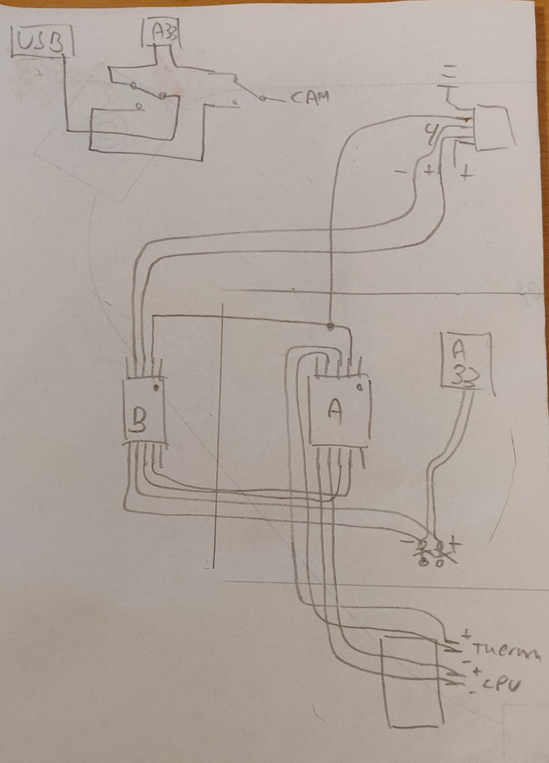
What we’re looking at is my ugly hand drawing, showing the two DPDT (Dual pole Dual throw) switches that allows us to cut the connection between the CPU and it’s devices. In this case we disconnec the USB port for charging and data and the Thermal Core and then reconnect these two devices so we’ll end up routing USB data from the Thermal core out the USB port, without the CPU internally doing any work.

We can handily do this since the 3.3V rail is alive when the camera charges. When the USB cable is plugged in for charging the display comes on, the charging symbol is shown and the screen is turned off again. Behind the scenes the CPU is still running (although in a low-power state i believe)

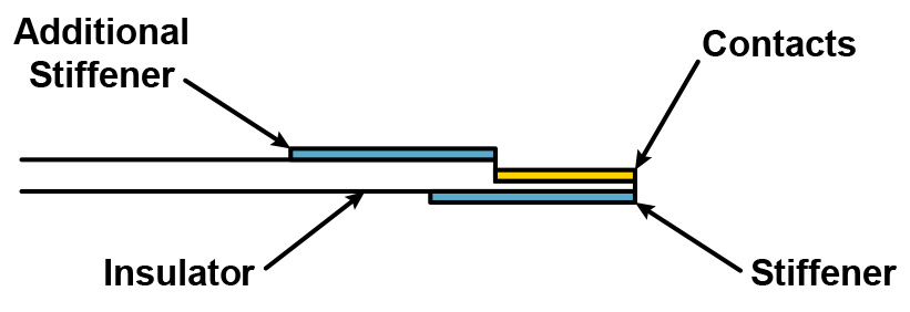
If you would rather look at a proper schematic i’ve drawn it up in KiCad for your pleasure as well. Be aware that i made a mistake in the schematic. The upper 1K resistor does not go to 3.3V. It goes from the ID-pin of the USB-plug to the SEL-signal on the chips, and from there to GND via another 1K resistor. This is to form a voltage divider and pulldown from the 5V USB to the chips that only support 3.3V!

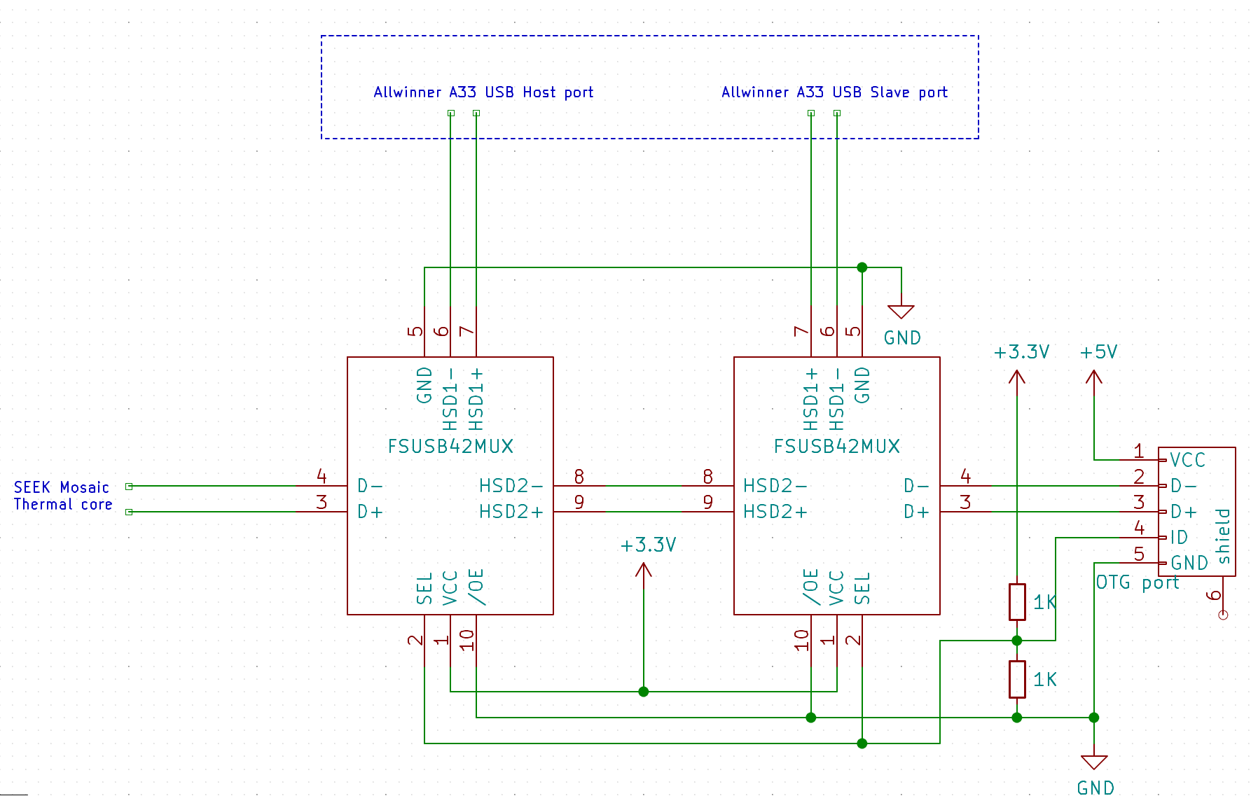
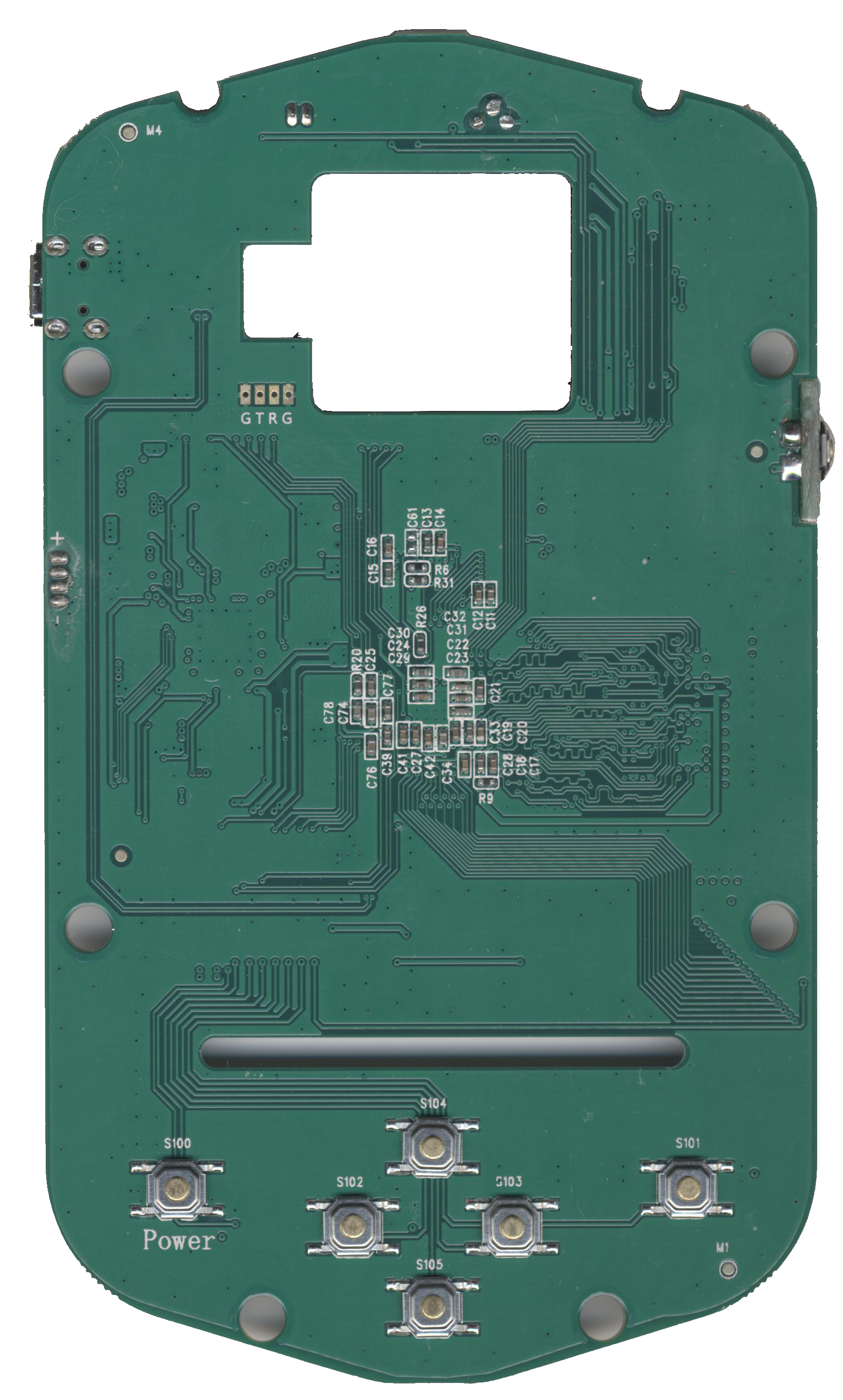
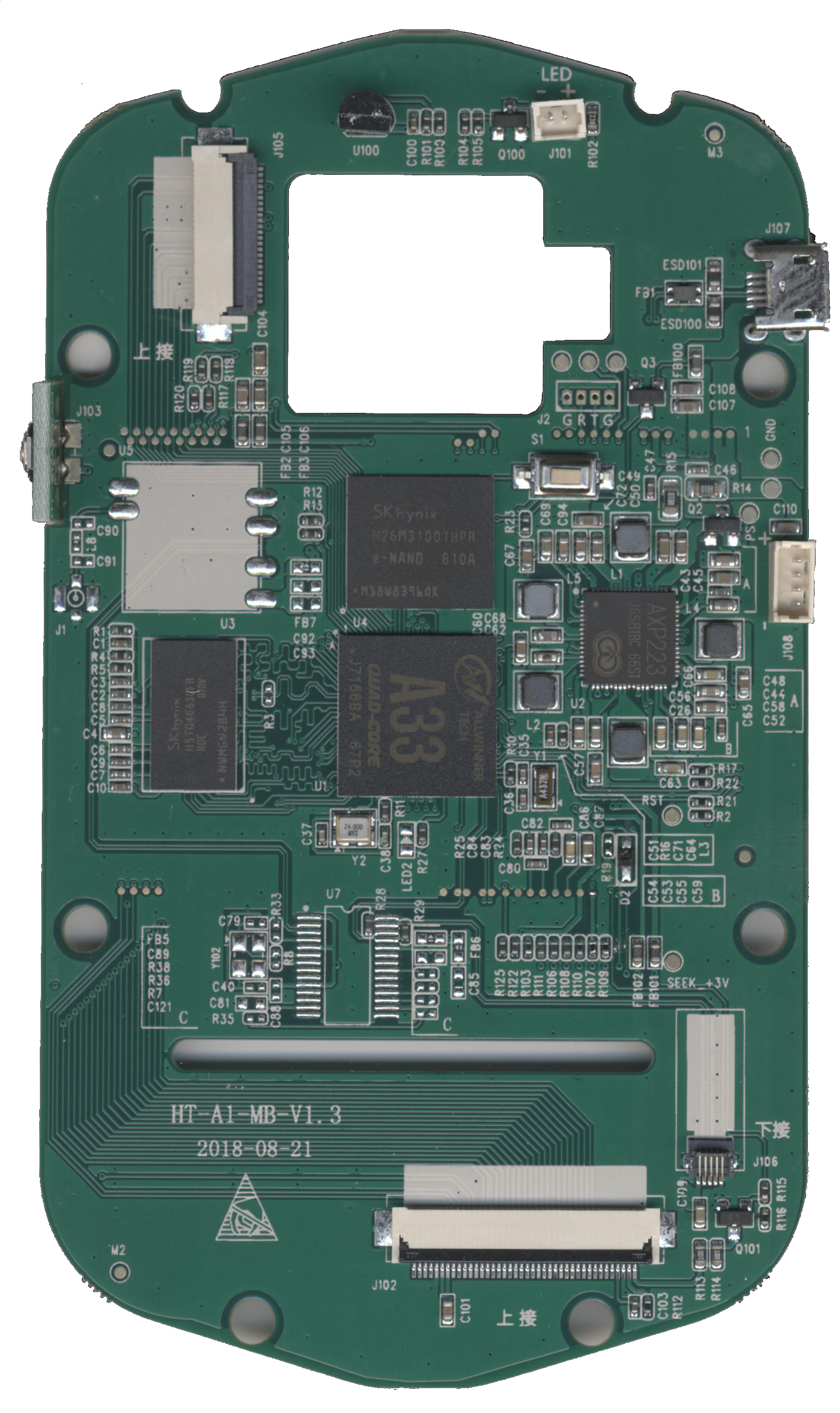
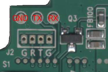
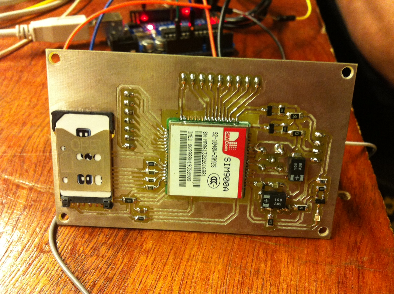
We need to cut the USB data stream on the PCB. There is some zero ohm resistors on the two data lines from the Thermal core to the CPU, situated where the GL850G USB HUB would have been situated (R28, R29). If i remove these i can access the data on what would have been pins 25-28. We also need to break the path on the lines from the USB connector for the outside world. This can be done just where the signals go from the bottom layer, trough a set of vias and to some testpoints. The solder mask is removed on the vias and the trace is cut between via and test points.

So if we switch these data lines around while the 3.3V rail is alive and the sensor has power we should be able to route the USB data out of the device.

But how do we trigger this? One could use a small micro processor and hook into the buttons and do something like holding down a key on the front while plugging in, that would enable the switch – but i went with a simpler solution. The fourth pin in the USB connector (the ID-pin) is not used in the HT-A1 so it’s open for playing around. If i make a custom OTG cable that goes from my phone to a micro USB plug with the ID pin pulled to +5V i can trigger the switch. This would allow me to plug the phone into a HT-A1 that is turned off. It will start charging and be immediately ready for the phone to initiate USB data transfers. Cool, huh!

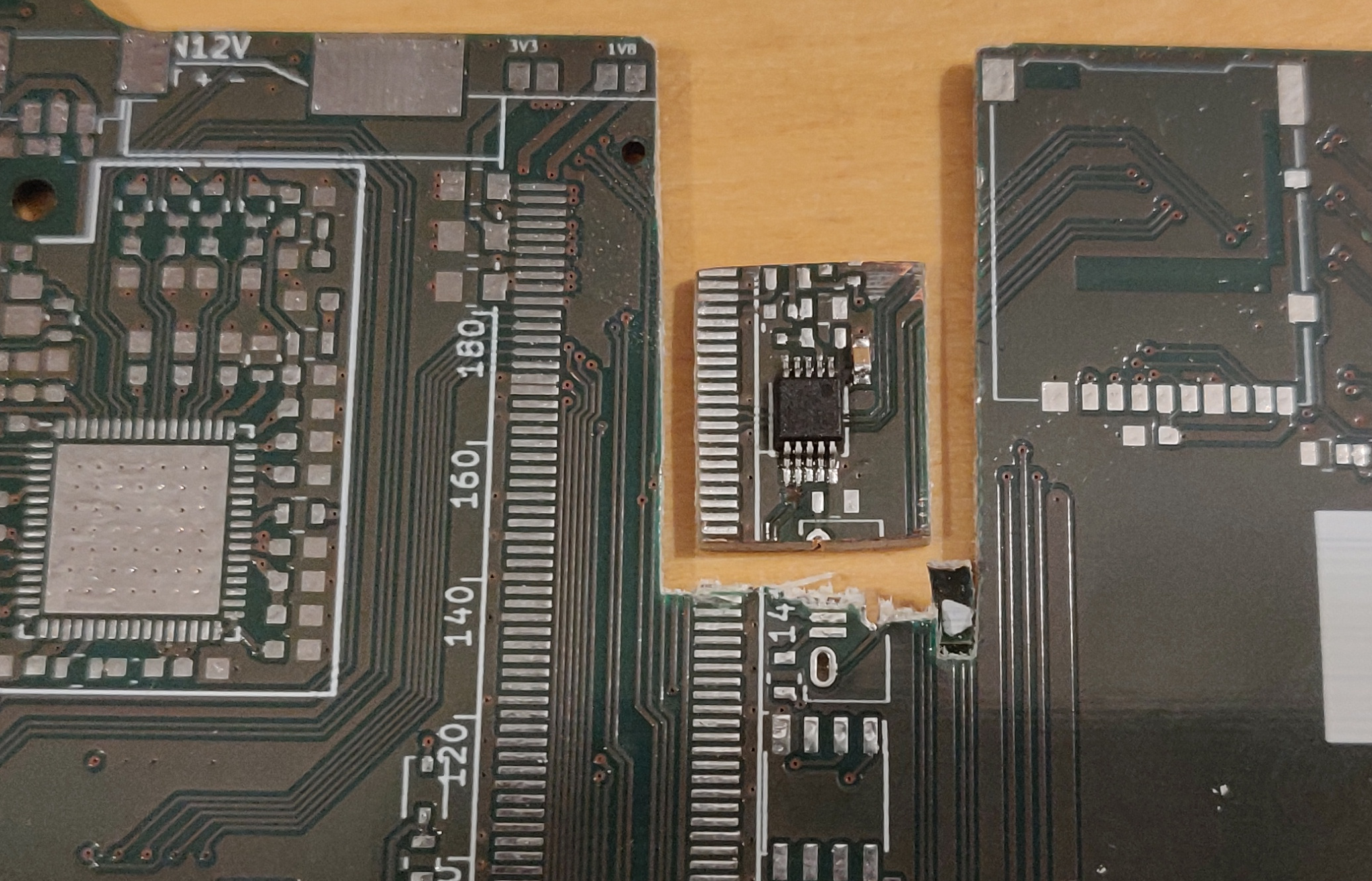
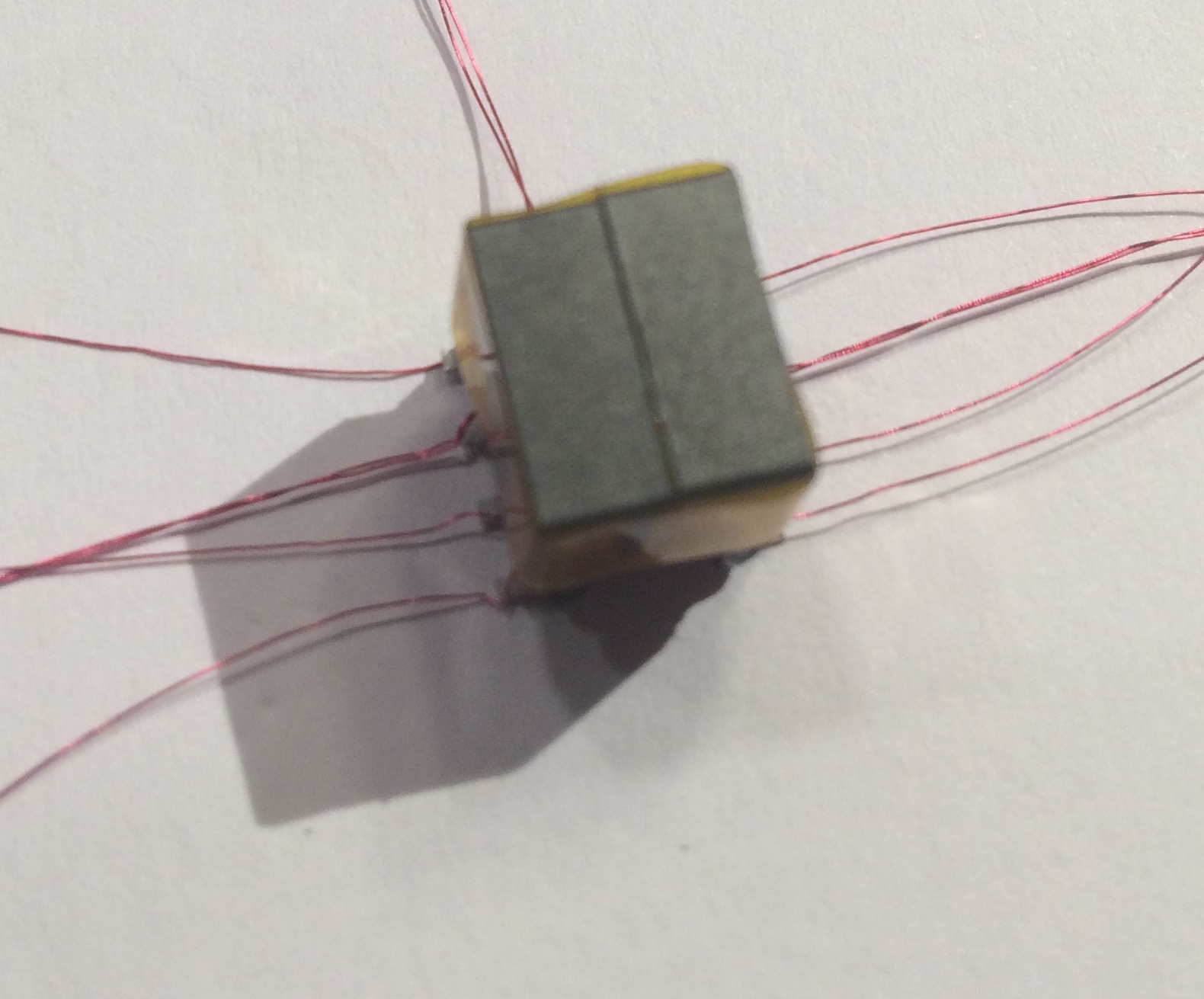
I have a bunch of scrapped circuit boards from my employer which employs some circuitry where a USB signal is switched around with an analog switch that is rated specifically for USB data signals, the FSUSB42

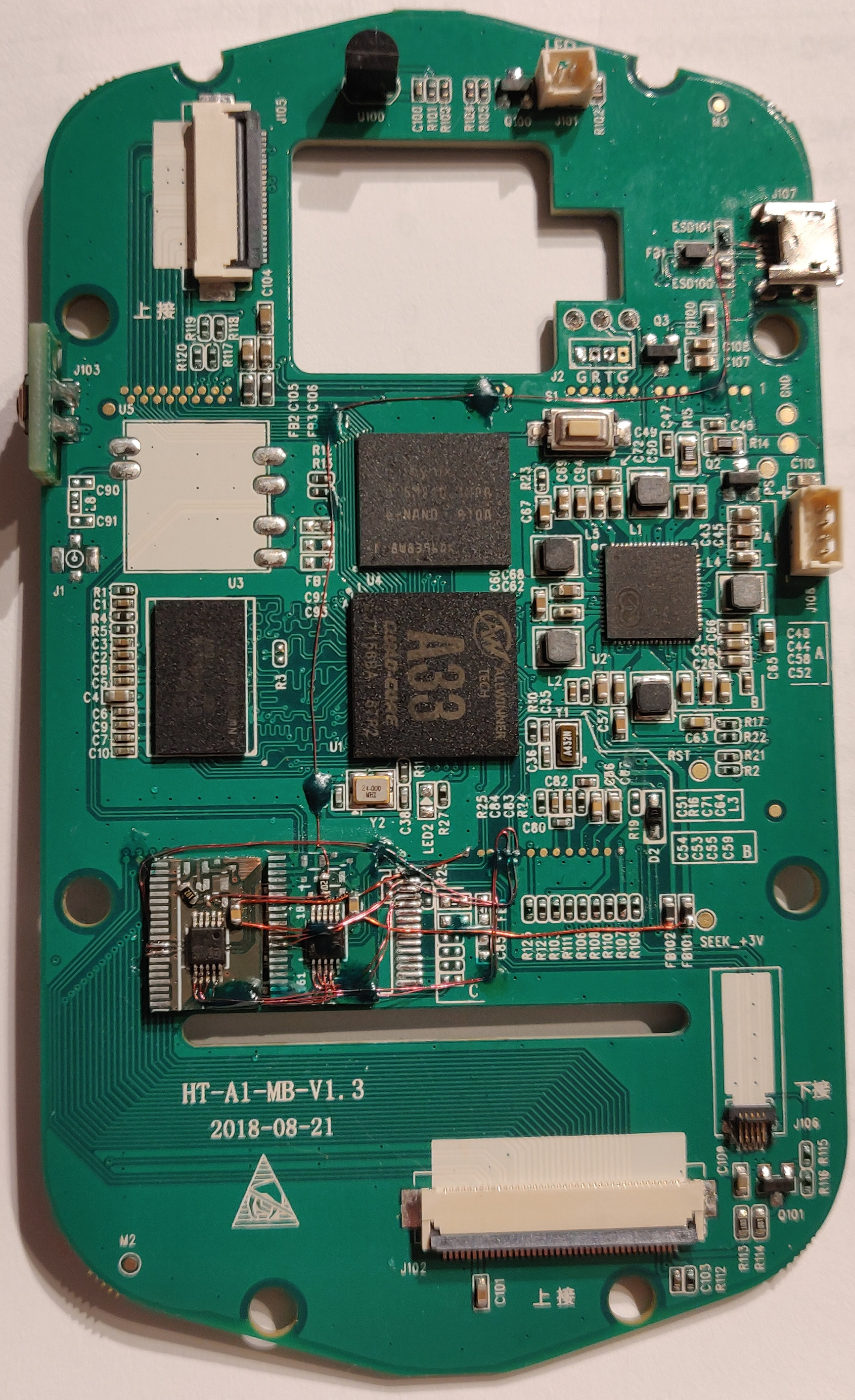
This chip comes in two variants. Piss annoying housing (UMLP) and just downright annoying housing (MSOP). Both are a chore to hand solder point-to-point so i got the idea to cut out a portion of the board with the chip. It’s not pretty but it sure gets the job done. There is oodles of place behind the mainboard so the extra couple of millimetres doesn’t really pose a problem.

So i took my trusty Goscut Eclipse 2000 plate shears and cut out the wanted portion of the PCB. I did this twice since i need two DPDT-switches.

So i took these two cutouts, placed them in a vacant spot on the mainboard and started wiring with enameled magnet wire. This is a great way to spend a Sunday evening btw – Just after easter lunch and a good long walk with friends in the city.

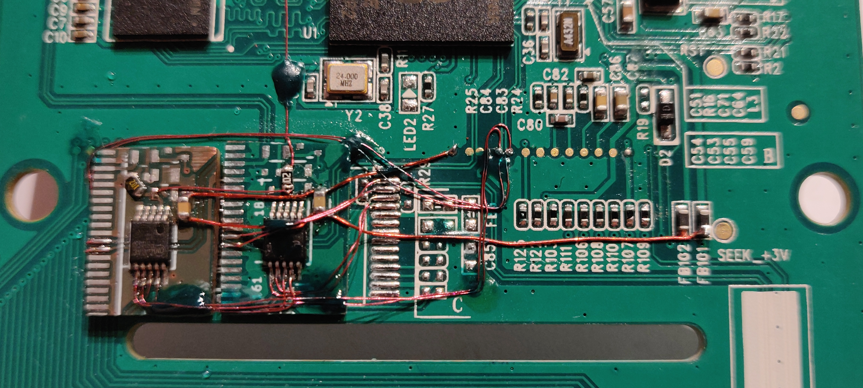
I use green UV-curing soldermask to hold the wires in place. Once i’ve placed a few wires i lock them down with a drop and cure the glue quickly with a 405nm laser pointer.

The finished article look like this. Not too bad if I must say:

The first sign of life on the phone 🙂
The finished setup. The cable is just a temporary one i made from some parts from the scrap bin

A weird thing i found – the image is upside-down. So i need to hold the HT-A1 upside down or my phone for it to be right-side up. I didn’t find any function in the app to rotate the image 180 degrees around. What do people do that have the dongle and USB-port in the top of the phone?

So where does this leave me? I need to solder a nice, short cable, preferably with some angled connectors so i can piggyback the phone on top of the HT-A1 and use it as a whole. I have some connectors and will probably just 3D-print some casings for it instead of waiting for the slow donkey from AliExpress.

On popular demand, i have desoldered the EEPROM in the Mosaic module and read out the firmware. The file is available in BIN and HEX format here

Any ideas, comments etc – you are very welcome to let me know what you think in the comment section below.

Dec 03

This is part 1 of my hacking adventures on the HT-A1. To see part 2, click here

After having tried to software-hack my old Flir E4 to get a higher resolution, and failed at that (some of them cannot be upgraded for unknown reasons), I was on the lookout for a better resolution device.

Having watched Julian Ilett’s video review of the device, steered me onto the cheap HTI (Dongguan Xintai Instrument Co.,Ltd.) HT-A1 thermal imager.

Almost all the other cheap off-brand imagers i have seen is pretty crap, but this one boasting a resolution of 220×160 pixels, that’s not half bad (compared to my old Flir E4, which was locked down at a measly 80×60 pixels.

Before  pushing the Order button, i went to do some more research and found this teardown video by Youtube user “The Equalizor“.

This reveals that the camera uses a sensor module from SEEK thermal and reveals some other nice details. Go see his video on how to get into the device.

It looked good, so i ordered one using the link on Julian’s video. After approx 3 weeks (whereas one week was it being stuck in customs) it finally arrived. I turned it on and checked that all worked, and then to continue to take it apart 😀

This is not a review, nor a teardown. This has been done before. I will look into what’s happening on the serial interface that is clearly evident on the board, and i will try to figure out what kind of communication protocol there is between the sensor and the mainboard.

The mainboard in all its gory details. All pictures are clickable for magnification.

Apparently the mainboard is a quite new revision (August 21, 2018), and not carrying a CPU-daughter board like on The Equalizor‘s camera.

Looking at the mainboard, trying to figure out how everything is wired together, it becomes apparent that there is a room for a module of some kind, denoted U5. Hmm, GPS-module for geotagging or WiFi-module? The traces going off to J1 with the antenna matching components screams WiFi to me. Who makes a WiFi-module in this approx. 12x12mm footprint? EDIT: I found it, using the right search words on AliExpress: “Tablet WiFi module” – It’s a module carrying the RTL8188CUS WiFi-chip.

What is interesting, when we follow the tracks from this missing U5 module, they go to a missing U7 chip. The data pair from the thermal module also goes here, but is jumpered by two 0Ω resistors (R28 & R29) … Hmm this smells a lot like USB! – What is U7 was a missing USB-hub? I’m thinking GL850G in SSOP-28 housing, a good old classic. A datasheet is available here: GL850G USB Hub 1.07.

So, we know that the thermal imager is running USB communication with the main Allwinner A33 CPU. No need to put the logic analyzer on these lines for hacking – we need to look at that serial port to see what’s happening on boot!

The cable between the sensor and the mainboard, Front and back view.

It carries GND, +3.3V and USB data.

The sensor module itself:

Front of the sensor has a removable lens, held in place with two daubs of what seemed to be hot-melt adhesive. It was easily removed with a scalpel. I am planning to design and 3D-print a tool that fits into the holes in the front to be able to set the focus.

The processor on the thermal module is the NXP LPC4330FET100, a Dual-core Cortex M4/M0 chip. More info here

The camera module is a sandwich of two boards – front board holding the directly bonded sensor (this is pure speculations)

Bottom side of main PCB with the NXP micro holds some support circuitry and a big SPI flash that holds the firmware that runs the module.

On top of the main board, in vicinity of the thermal module there is U100, it’s a bog-standard DS18B20 thermometer for local compensation of the camera’s own temperature. I guess the thermal module does not carry its own temp. sensor.

Some playing around with booting the board without thermal imager or visible camera modules revealed that with both unplugged it will hang indefinitely at the boot screen (but it will still switch off when you press the power button, so it’s not dead behind the scenes). Unplugging only one of the cameras/sensors will have the camera booting happily. Unplugging the visible camera makes all mixed image modes go black. Unplugging the thermal module makes all thermal readings go away, but you can still use the visible module just fine. I guess it was built this way to not die completely if one of the devices went bad, but instead would boot and the user could see what was missing, to go report the error and get the device off for repair.

On the back of the board there is a switch, S1. I tried pressing it while the unit is in operation, no response.

Holding it down while pressing power button yields a device that does not boot, but rather “locks up” – I’m pretty sure this button is to go into some bootloader flash mode. The firmware talks about a “fel button” – it’s for firmware flashing as far as i know for now.

Well this is getting interesting!

The small connector footprint J2 showed to contain no output at all, i scoped it and it’s dead as a dodo.

The three test pads over it on the other hand is alive and well with debug serial@115200 8N1 – YEAH!

Booting the camera with all devices connected will yield this nice bootlog:

HELLO! BOOT0 is starting!
boot0 version : 3.1.0
reg_addr 0x01f00100 =0x00000000
reg_addr 0x01f00104 =0x00000000
reg_addr 0x01f00108 =0x00000000
reg_addr 0x01f0010c =0x00000000
reg_addr 0x01f00110 =0x00000000
reg_addr 0x01f00114 =0x00000000
DRAM DRIVE INFO: V1.5
DRAM CLK =552 MHZ
DRAM simple test OK.
dram size =512
card boot number = 2
card no is 2
sdcard 2 line count 0
[mmc]: mmc driver ver 2014-07-07 16:54
[mmc]: ***Try SD card 2***
[mmc]: mmc 2 cmd 8 timeout, err 0x00000100
[mmc]: mmc 2 cmd 8 err 0x00000100
[mmc]: mmc 2 send if cond failed
[mmc]: mmc 2 cmd 55 timeout, err 0x00000100
[mmc]: mmc 2 cmd 55 err 0x00000100
[mmc]: mmc 2 send app cmd failed
[mmc]: ***Try MMC card 2***
[mmc]: MMC ver 4.5
[mmc]: SD/MMC Card: 4bit, capacity: 3728MB
[mmc]: vendor: Man 0x0090014a Snr 0x012084b9
[mmc]: product: H4G2a
[mmc]: revision: 1.1
[mmc]: ***SD/MMC 2 init OK!!!***
sdcard 2 init ok
The size of uboot is 0x000bc000.
sum=0x0ccccd69
src_sum=0x0ccccd69
set_mmc_para,sdly 50M 0
set_mmc_para,sdly 25M 0
Succeed in loading uboot from sdmmc flash.
Ready to disable icache.
Jump to secend Boot.
[ 0.335]

The rest is not shown here, open BOOT down here under to see the full bootlog.

Raw logs from boot can be found here – some of them is booting without imagers connected, just to see how it reacts:

BOOT

NOTHERMAL_BOOT

NOVISUAL_BOOT

NOTHERMAL+NOVISUAL_BOOT

System is running Busybox, and with some serial debug magic i managed to copy files from system folders to the /mnt/IMGS folder that is exposed over USB. I found all kind of good stuff there – in /boot/ i found logos for other manufacturers (different branding), the cheesy battery recharge-animation – even audio files though the system has no way of doing audio recording or playback 😀


Now, making a new boot logo/animation is next, i think!

Yep, it had to happen: Video of new bootlogo i made in a hurry

I took at backup of the system partitions, and you can get them here:

Data partitions

I decided to order in a WiFi-module and USB-Hub-chip so i can enable WiFi and SSH-access on this 🙂

— I will update this when the parts arrive.

Aug 10

The usual trashpicking yielded a nice HP Envy 4500 AIO with missing top cover on the flatbed scanner.

Before just ripping it to pieces, i wondered how good the WiFi-support/setup was regarding the scanner, so i got it going. It complained about empty cartridges (no surprise here) but eventually i got to setup menu, enabled WPS and got it connected to my home WiFi.

My Mac immediately found it and installed it via Bonjour/AirPrint – no drivers needed (or i already had it on the system)

Scanning seemed to work just fine, so now i was wondering. Could the printer mechanism be discarded and the printer turned into a WiFi-enabled scanner?

First try: Disconnect FFC to the print carriage, boot printer and see what happens. Well, it was not happy. I got an error message in a rather crude font, so it died pretty much early in the boot process, before the “GUI” was up.

So apparently, it needs to talk to the de-serialiser/buffer chip on the carriage. I plugged the cable back in, removed the cartridges and tried again. This time it booted all the way and got onto WiFi. Scanner was still fully usable – Yay!

Next cause of action was to remove that stupid “lid open”-sensor. It’s just an opto-fork on the back side of the control/LCD/panel. Desoldering it from the board will keep it happy (there is a pullup on the receiving phototransistor inside it, so with the component missing, it looks like it’s in darkness – e.g. the lid is closed on the printer).

So, how much else can be unplugged you ask? Well, pretty much everything!

I unplugged cables for “cleaning station”, paper encoder, the two DC-motors and it still booted up – i got a shitload of error messages when doing this, but WiFi still works.

Now i’m pretty long in the modification process, and i come to think of – how do i set this up for a new WiFi-network some other day? – Pressing the buttons on the LCD control panel is of no help. Error messages keep popping up faster than i can navigate the menu – F*ck!

Plugging in back all the stuff yielded me with “No cartridges found” instead of the dreaded “Carriage is stuck” – but still no way to access the menu. At this point i had taken apart the carriage and removed all the mechanics and only kept the PCB with flex cables – so no plugging in back the cartridges!

Then i came to wonder – can you setup WiFi from the software/driver on the computer? – Oh yes you can – Even if your printer is completely bonkers and is reporting more errors than you can count to!

So connecting the printer via USB, and messing around in drivers control panel, calling up the Toolbox, i was able to scan for WiFi-networks, and connect to one. Success!

So now i have the machine pretty much sorted out. All the printer mechanism is gone, only the small PCB with the De-serialiser/Buffer is needed. I ripped off the flex cable to the cartridges, desoldered the electrolytic cap and the encoder for the optical strip.

The original FFC from carriage to main board was rather long, so i went into my box of assorted ones to hunt for a shorter replacement. Shortly after i found out the cable i needed was a “flipped” cable – the connections on each end of the FFC is on each side of the cable. I couldn’t find a short cable that was flipped.

I found a reasonable short cable, ripped off the stiffener at the end, cut the cable clean off, and scratched the “back side” of the cable with a knife until the tracks appeared. The stiffener was glued back onto the other side of the cable, and then i had a short, flipped FFC.

The boards was arranged and put on top of each other with some hot glue.


The resulting parts were again hot-glued to the bottom of the scanner case.


Final touch would be some 3D-printed feet so it can sit flat on a table. Right now it’s a bit uneven on the bottom because of the power supply in the front right corner.

I hope this inspired you to do some hacking on your own – Personally i really had no need for an WiFi-enabled scanner. I already have a fine scanner with ADF and all the bells and whistles, but this afternoon project was more like I’ll hack it just because i can!

Oct 16

While attending the 2017 edition of Mini Maker Faire at Aarhus central library (DOKK1) We (Labitat expedition) also went to the obligatory visit at OSAA (Open space Aarhus) and looted some stuff from their Limbo-shelves.

In between all the good stuff there, I found a Sony BDP-S360 BluRay-player. It went back home for exploring.

Upon powering-up it just sits there saying “Wait” on the VFD while making some mechanical noises.

As I have no interest in having a BD-player it was turned into parts. Nothing really useful was found inside. Bog-standard primary SMPS, 22 watts max output and mainboard with more or less single-chip-solution.

The mechanics had the old venerable KES-410-optical pickup (known from the ‘PS3 fat‘)

As I have a special interest in VFD’s (Vacuum Fluorescent Displays) (amongst other older display technologies) I took a closer look.

BDP-S360 VFD Front panel

It has all the power supply circuitry onboard directly – usually the Filament-drive and VEE-supply is built-in in the main SMPS, but Sony apparently went for the simpler approach here. I like that!

2 minutes on Google yielded the service manual with nice schematics and pictures of the front panel-board foil and silkscreen.

Looking at the schematic for the power supply for the VFD it’s pretty bog standard-kinda-deal here.

Transformers have always been an interesting item – for most a “black box”. I would like to know the number of windings etc. So i took out the transformer, put it into Acetone for a minute and opened the core (the outer ring lifts off, revealing the windings.)

BDP-S360 VFD Transformer pinout

BDP-S360 VFD Transformer opened up BDP-S360 VFD Transformer bottom view

I documented my findings here, in case that it might come in handy for someone else hacking with VF-Displays


T701:
Circular core, 10 pins.
Primary, pins 2,3,4
Feedback, pins 5,6
Secondary, VEE 1,10
Secondary, Filament 7,8,9
Tested at 160kHz
Primary inductance (end-to-end)    70 uH
Feedback inductance 2.2nH
Secondary, VEE 140uH
Secondary, filament 3uH
Winding order:
15+15 Windings 2-3-4 0.1mm
3+3 Windings 7-8-9 0.1mm
44 Windings, 10-1 0.1mm
5 Windings, 5-6 0.1mm
Voltages measured:
VEE is -18V
Filament supply is 5.4Vpp running on a -13.7V bias
Switching circuit runs at 216 KHz
The VFD-glass itself seems to be custom-part with special symbols for BD-player. I couldn’t find anything online on it.
The controller on board is the old and venerable PT6315. It uses a 3-wire interface and is very easy to interface with.
I will keep the board and parts for some more fun another day.
Update:
For kicks i tried making my own transformer on a EP-7 core with PC40-material.
Same number of turns, 0.1mm airgap (2 layers of Kapton tape)
Slightly higher output voltages, same switching frequency.
Jul 27

arduino-yun-front

The newest addition to my swarm of never ending pile of interesting electronics is the Arduino Yún.

As I was getting some parts from Newark Canada, I just thought, well i’ll get myself an Yún to play with as well.

Yún means Cloud in Mandarin, so it’s quite obvious it is an Arduino meant to be connected to the cloud (Internet of Things).


As I usually do, I hack into the deeper workings of devices, and in the case of the Yún, there will be no difference.


I will dig deeper into it’s internals – have You ever seen the “Black magic” hiding under the shield? I haven’t.

Also, later I will look into how much power this unit takes, and to see if there is any way to tweak the power usage.


Setting up the Yún was a breeeze – I followed the instructions over at http://arduino.cc/en/Guide/ArduinoYun

Quickly I had it connected to my own WiFi-network, and programming it over Wifi with Arduino 1.5.7 (Beta at the moment) worked quite nicely.


Well, let’s get to the point, what exactly is hiding under that EMI-shield?

A quick desolder job with the Solder-wick (Chemtronics 10-100L, the best money can buy!) and the cover was off.

Yun uncovered - overview

Yun uncovered – overview


Aha! – three chips – that ain’t much.

On the left we have a Winbond W9751G6KB-25 Р16 Bit DDR2-RAM Рthis is the main memory for the DD-WRT linux-environment that the Y̼n runs.

In the center there is the Atheros  AR9331-AL1A Wireless SOC – This is where all the magic happens.

And on the Right, once again from Winbond, a 25Q128FVSG – a 128 MegaBit Boot-flash, using SPI-interface.


So, now you know what hides under the shield, and you do not need to void the Warranty on your Yún to find out 😀

– Due to time constraints, I will leave the power-measurements to the next blog-post, as I need some time to gather readings, and present them in a usable manner.

Apr 23

I got my sticky hands on some very nice vintage LED-displays, and some days ago i got a pack of nice prototype-PCB’s from eBay, so of course i had to make two small test-boards for these displays 😀

This one is for 4 pcs. of TIL311, intelligent Hexadecimal display (shows 0-9, A-F)

TIL311 LED Display

TIL311 LED Display


The next board is for a DL1416 display. It can display all numbers and some Alphanumeric digits. It has a 7-bit Data-bus.

DL1416 LED display

DL1416 LED display


The plans for them? Well i have enough of both types to warrant the time needed to layout a design for a very limited-edition wristwatch 🙂

Nov 23

EDIT: Read bottom of post!

I have been toying around with GSM modems for some time – working on the Rotary Cellphone project, i settled on the SIM900-module from SIMCOM.

Milled SIM900-board

Early in my quest, i mistakenly read, that the SIM900 was Quad band, and the SIM900A was Dual band. As I decided that i did not need the Quad-band capability, i ordered the SIM900A-modem, as it was a few $ cheaper.

Ordering the first module from far east (AliExpress) my choice was the SIM900A model. I milled a breakout-board for the GSM-module, soldered it on, and everything “seemed” to work, but i could not register the modem on the Danish GSM-network. It acted like it was locked to a specific GSM-vendor.

The modem being brand new, ruled out the option that someone else had a go at it, so what was happening ?

I trawled the documentation at SIMCOM, and couldn’t readily find any information on what the differences between a SIM900 and a SIM900A-model were.

Some helpful people at the local Hackerspace mailing-list soon found the culprit (i guess their Google-fu was better than mine)

The SIM900A-model is locked to these regions:

  • China
  • India
  • Singapore
  • Malaysia
  • Thailand
  • Indonesia
  • Cambodia
  • Vietnam
  • Laos
  • Burma
  • Brunei
  • Philippines
  • East Timor

Official documentation is mirrored here: SIM900A Supported MCC List V1.00

Why SIMCOM makes this module, locked to specific regions, i do not know, if you have any idea why, please leave a comment.

User [] had luck upgrading the Firmware on his module – you can read about his findings here – i have not tested the firmware file, as i destroyed my 900A-model in frustration and anger.

Jul 13

Finally got time to shoot a vide of the cube working, what do You think ?

Feb 08

First initial testing, after fixing some minor errors i made in the layout (Swapped RX/TX, not first time) and swapped D & S on the Fets. Grrr…

Feb 04

I’m in the process of building a 5x5x5 LED Cube like many others. The firmware is designed by [SiGNOUT] and [knielsen] from the local Hackerspace.

Their Cubes use a Seperate Arduino, and TLC5940 LED-drivers in TSOP housing. I would like to push the limits on my version of it, so i ordered the TLC5940 and Atmega328P in the smallest possible cases available. I would like to try BGA some day, but BGA requires more than dual layer PCB, so that’s impossible without professional PCB’s. The Atmel is 4mm² and the TLC5940 is 5mm².

The board is 2-layer and has holes through plated chemically. It is made on our Protomat & Minicontac II.

Here’s some pictures of the milled PCB:

Some more pictures in the Gallery

There’s pictures of another PCB in the folder, an Infrared LED exposure device for Playing with a Laser printer.