This is part 2 of my hacking adventures on the HT-A1. To see part 1, click here
Mounting the USB-hub and WiFi-module never came to be (i lost interest and figured it would be hard to add the missing features in software since i’m no expert at embedded linux and i don’t have the sources for the software the camera is running.
Browsing the internet it became apparent that Seek is now officially stating that they sell OEM modules and you can buy a development kit with SDK etc. I had a look at their pictures and it was clear that the module that the HT-A1 is using a variant of their “Mosaic” thermal core.
Now, what happens if i load the Seek app and connect this to my smartphone? Will the app recognise the module?
Well only one way to find out i think. I found a suitable piece of flat flex cable that handily went from the 0.5mm pitch to 1mm pitch (so soldering would be a tad easier) I cut it to size so it would fit the small 5 pin connector on the Mosaic core. The docs from Seek says that the Mosaic core is good from 3.3 to 5.5V. I didn’t immediately saw any reasonably sized voltage regulator on the module from the HT-A1 so instead of taking any chances i put two standard 1N4007 diodes in series with VCC to drop the voltage to 3.6V.

I made a concoction of this custom cable and an USB-C OTG cable that would plug into my Oneplus 6-phone.

I went into settings on Android and turned on OTG support so the port would supply power, plugged in the cable and was met with a friendly popup asking if i would allow Seek Thermal to access PIR206 Thermal Camera? – Hell yes!
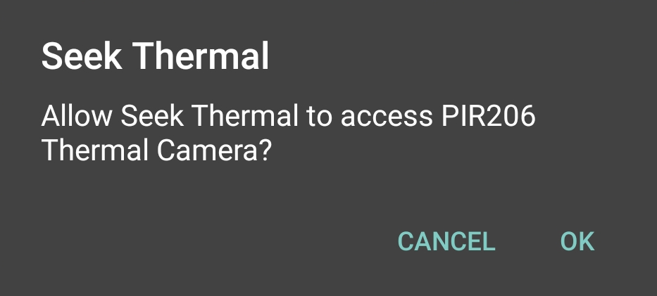
Pressing OK, nothing more happened. I opened up the Seek app and in the top it said “Unknown” as connected. Pressing the name opened up the preview – it works 😀

OK. This is awesome. Now i can actually use the thermal core in my HT-A1 to record videos via the app.
I don’t want to gut the HT-A1 since i really like have dedicated hardware for a job – that was also the reason i went with the HT-A1 instead of a Seek dongle or similar device that plugs into a phone. I don’t want to leave my phone in a test setup etc, or even worse having a product that eventually gets obsoleted because the app isn’t updated anymore. I could see that happeing very well if you had one of these for an iPhone.
But not having the possibility to record video really detracted from the dream of having the dedicated hardware.
So how do i connect the Thermal core to my phone without drilling any extra holes in the HT-A1 case and installing extra plugs and switches? With some trickery of course!
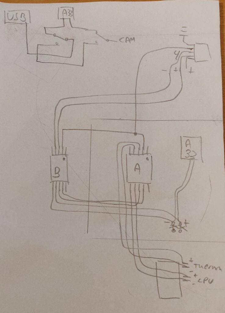
What we’re looking at is my ugly hand drawing, showing the two DPDT (Dual pole Dual throw) switches that allows us to cut the connection between the CPU and it’s devices. In this case we disconnec the USB port for charging and data and the Thermal Core and then reconnect these two devices so we’ll end up routing USB data from the Thermal core out the USB port, without the CPU internally doing any work.
We can handily do this since the 3.3V rail is alive when the camera charges. When the USB cable is plugged in for charging the display comes on, the charging symbol is shown and the screen is turned off again. Behind the scenes the CPU is still running (although in a low-power state i believe)
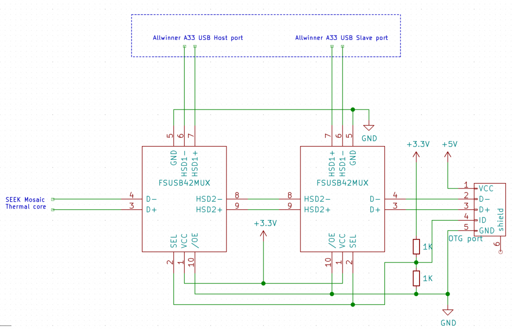
If you would rather look at a proper schematic i’ve drawn it up in KiCad for your pleasure as well. Be aware that i made a mistake in the schematic. The upper 1K resistor does not go to 3.3V. It goes from the ID-pin of the USB-plug to the SEL-signal on the chips, and from there to GND via another 1K resistor. This is to form a voltage divider and pulldown from the 5V USB to the chips that only support 3.3V!
We need to cut the USB data stream on the PCB. There is some zero ohm resistors on the two data lines from the Thermal core to the CPU, situated where the GL850G USB HUB would have been situated (R28, R29). If i remove these i can access the data on what would have been pins 25-28. We also need to break the path on the lines from the USB connector for the outside world. This can be done just where the signals go from the bottom layer, trough a set of vias and to some testpoints. The solder mask is removed on the vias and the trace is cut between via and test points.
So if we switch these data lines around while the 3.3V rail is alive and the sensor has power we should be able to route the USB data out of the device.
But how do we trigger this? One could use a small micro processor and hook into the buttons and do something like holding down a key on the front while plugging in, that would enable the switch – but i went with a simpler solution. The fourth pin in the USB connector (the ID-pin) is not used in the HT-A1 so it’s open for playing around. If i make a custom OTG cable that goes from my phone to a micro USB plug with the ID pin pulled to +5V i can trigger the switch. This would allow me to plug the phone into a HT-A1 that is turned off. It will start charging and be immediately ready for the phone to initiate USB data transfers. Cool, huh!
I have a bunch of scrapped circuit boards from my employer which employs some circuitry where a USB signal is switched around with an analog switch that is rated specifically for USB data signals, the FSUSB42
This chip comes in two variants. Piss annoying housing (UMLP) and just downright annoying housing (MSOP). Both are a chore to hand solder point-to-point so i got the idea to cut out a portion of the board with the chip. It’s not pretty but it sure gets the job done. There is oodles of place behind the mainboard so the extra couple of millimetres doesn’t really pose a problem.
So i took my trusty Goscut Eclipse 2000 plate shears and cut out the wanted portion of the PCB. I did this twice since i need two DPDT-switches.
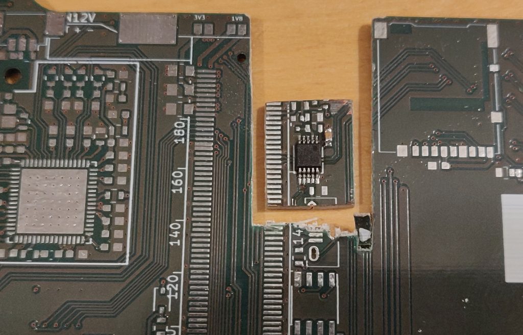
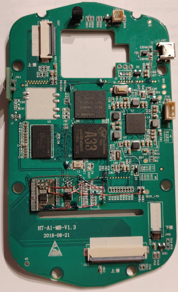
So i took these two cutouts, placed them in a vacant spot on the mainboard and started wiring with enameled magnet wire. This is a great way to spend a Sunday evening btw – Just after easter lunch and a good long walk with friends in the city.
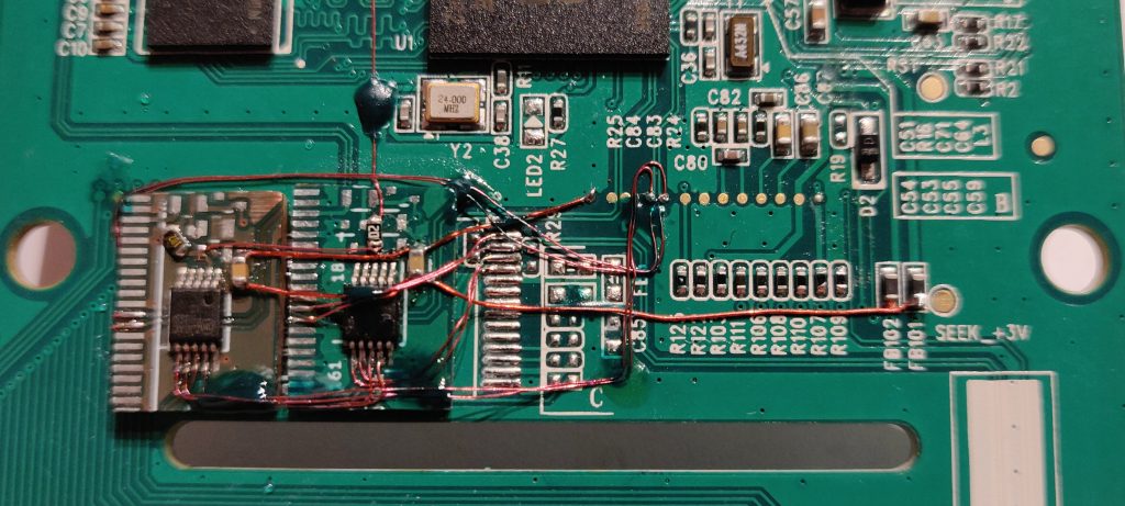
I use green UV-curing soldermask to hold the wires in place. Once i’ve placed a few wires i lock them down with a drop and cure the glue quickly with a 405nm laser pointer.
The finished article look like this. Not too bad if I must say:
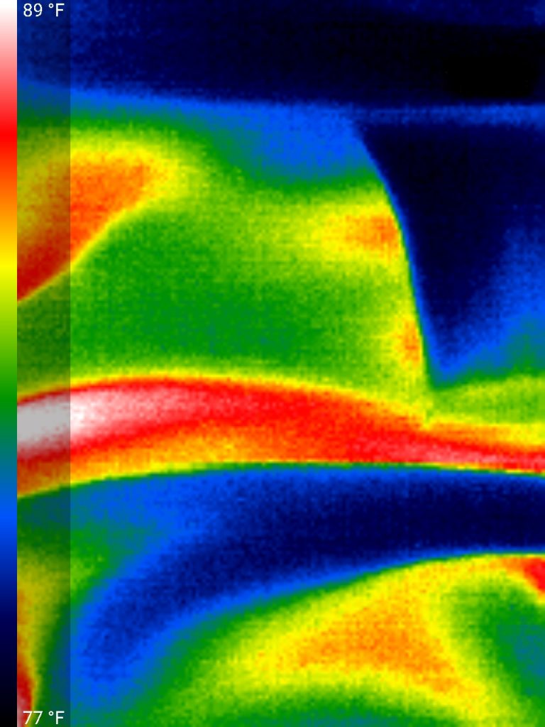
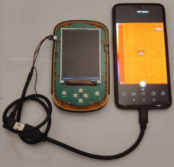
A weird thing i found – the image is upside-down. So i need to hold the HT-A1 upside down or my phone for it to be right-side up. I didn’t find any function in the app to rotate the image 180 degrees around. What do people do that have the dongle and USB-port in the top of the phone?
So where does this leave me? I need to solder a nice, short cable, preferably with some angled connectors so i can piggyback the phone on top of the HT-A1 and use it as a whole. I have some connectors and will probably just 3D-print some casings for it instead of waiting for the slow donkey from AliExpress.
On popular demand, i have desoldered the EEPROM in the Mosaic module and read out the firmware. The file is available in BIN and HEX format here
Any ideas, comments etc – you are very welcome to let me know what you think in the comment section below.