This is part 1 of my hacking adventures on the HT-A1. To see part 2, click here
After having tried to software-hack my old Flir E4 to get a higher resolution, and failed at that (some of them cannot be upgraded for unknown reasons), I was on the lookout for a better resolution device.
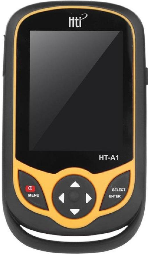
Having watched Julian Ilett’s video review of the device, steered me onto the cheap HTI (Dongguan Xintai Instrument Co.,Ltd.) HT-A1 thermal imager.
Almost all the other cheap off-brand imagers i have seen is pretty crap, but this one boasting a resolution of 220×160 pixels, that’s not half bad (compared to my old Flir E4, which was locked down at a measly 80×60 pixels.
Before pushing the Order button, i went to do some more research and found this teardown video by Youtube user “The Equalizor“.
This reveals that the camera uses a sensor module from SEEK thermal and reveals some other nice details. Go see his video on how to get into the device.
It looked good, so i ordered one using the link on Julian’s video. After approx 3 weeks (whereas one week was it being stuck in customs) it finally arrived. I turned it on and checked that all worked, and then to continue to take it apart 😀
This is not a review, nor a teardown. This has been done before. I will look into what’s happening on the serial interface that is clearly evident on the board, and i will try to figure out what kind of communication protocol there is between the sensor and the mainboard.
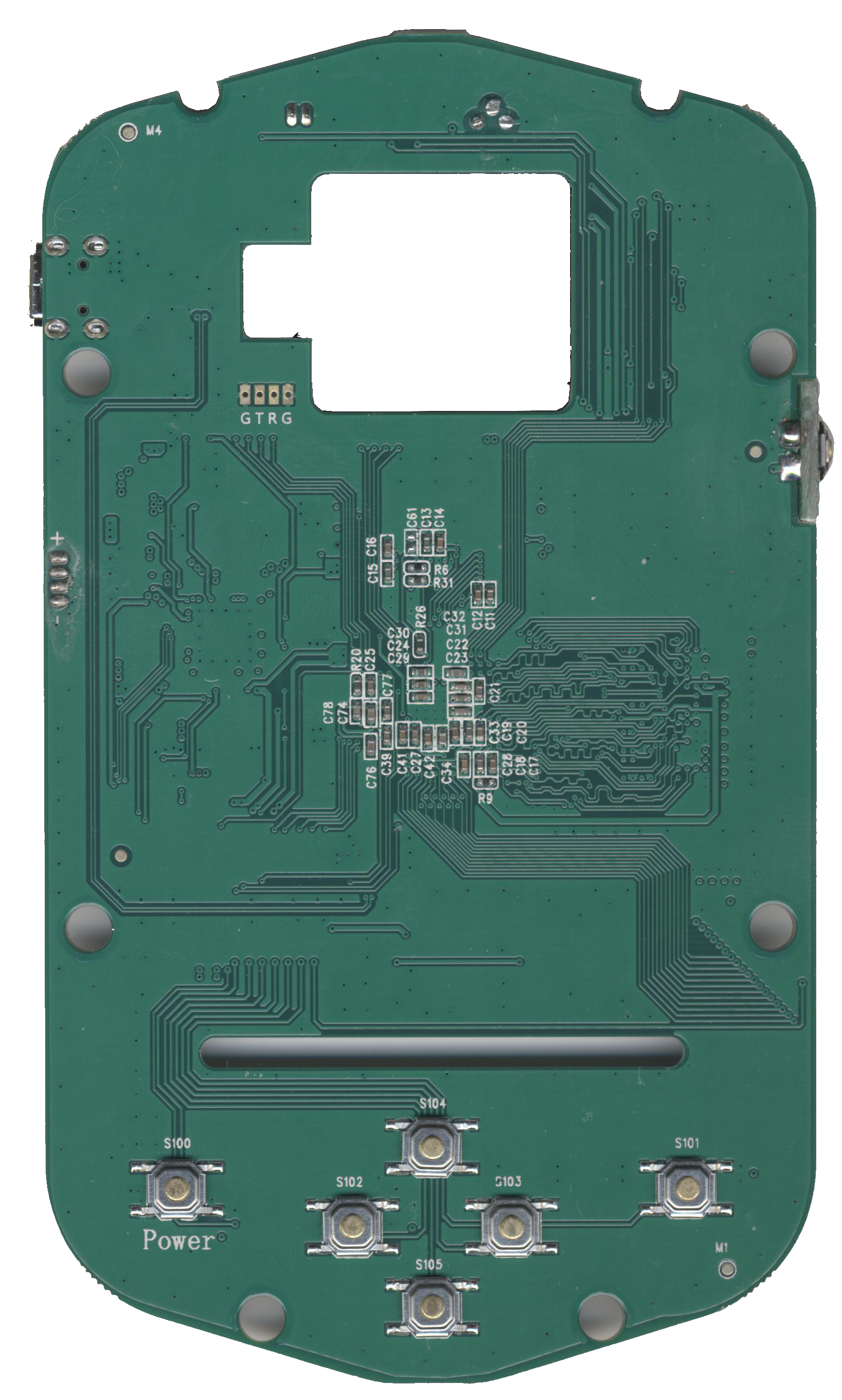
The mainboard in all its gory details. All pictures are clickable for magnification.
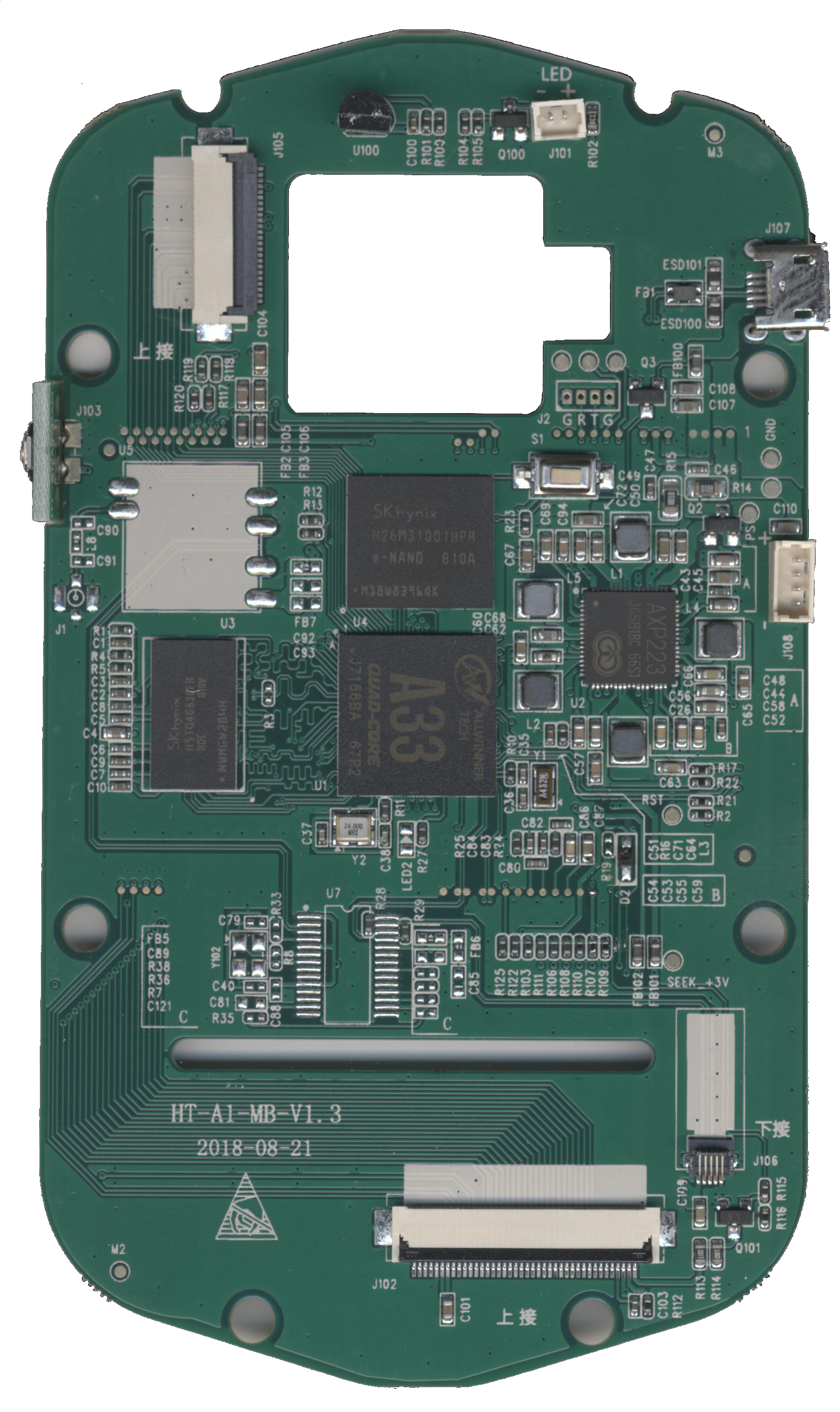
Apparently the mainboard is a quite new revision (August 21, 2018), and not carrying a CPU-daughter board like on The Equalizor‘s camera.
Looking at the mainboard, trying to figure out how everything is wired together, it becomes apparent that there is a room for a module of some kind, denoted U5. Hmm, GPS-module for geotagging or WiFi-module? The traces going off to J1 with the antenna matching components screams WiFi to me. Who makes a WiFi-module in this approx. 12x12mm footprint? EDIT: I found it, using the right search words on AliExpress: “Tablet WiFi module” – It’s a module carrying the RTL8188CUS WiFi-chip.
What is interesting, when we follow the tracks from this missing U5 module, they go to a missing U7 chip. The data pair from the thermal module also goes here, but is jumpered by two 0Ω resistors (R28 & R29) … Hmm this smells a lot like USB! – What is U7 was a missing USB-hub? I’m thinking GL850G in SSOP-28 housing, a good old classic. A datasheet is available here: GL850G USB Hub 1.07.
So, we know that the thermal imager is running USB communication with the main Allwinner A33 CPU. No need to put the logic analyzer on these lines for hacking – we need to look at that serial port to see what’s happening on boot!
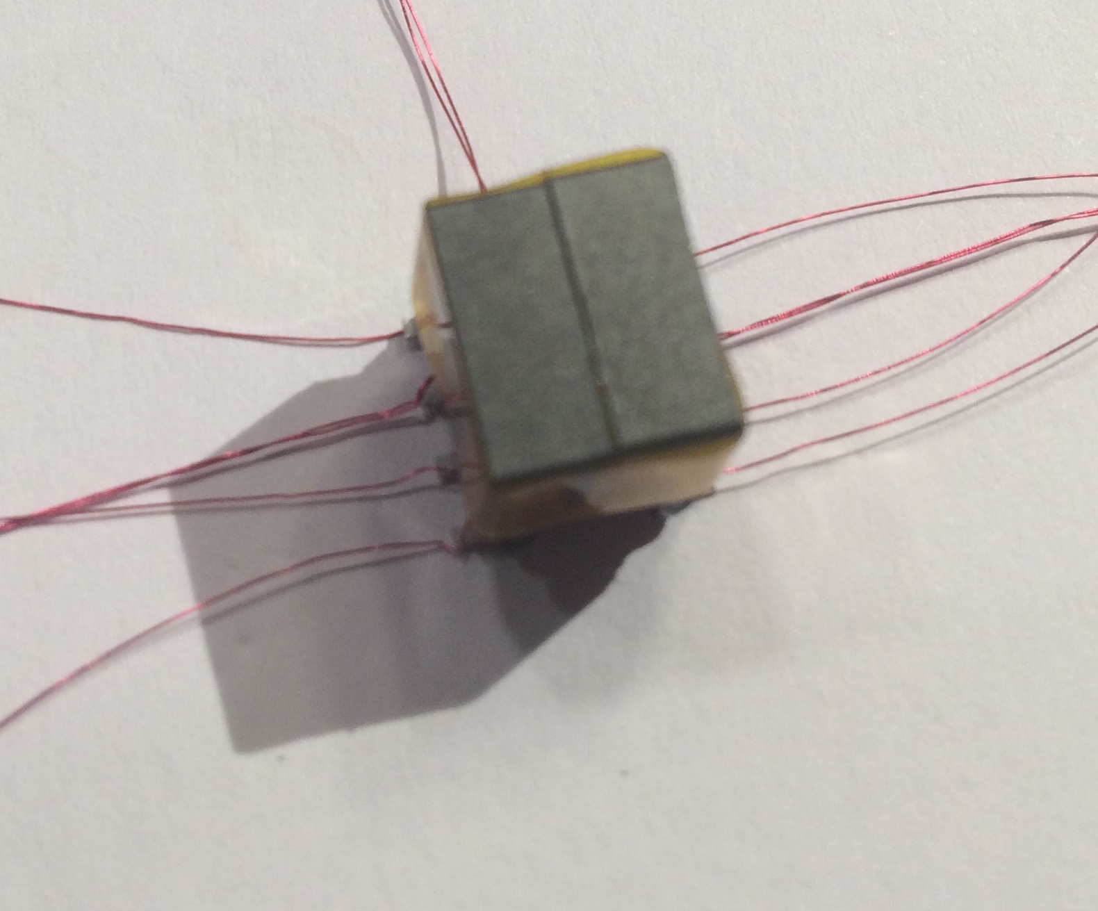
The cable between the sensor and the mainboard, Front and back view.
It carries GND, +3.3V and USB data.
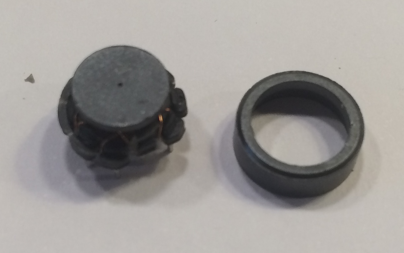
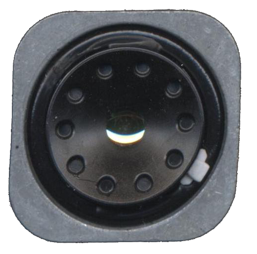
The sensor module itself:
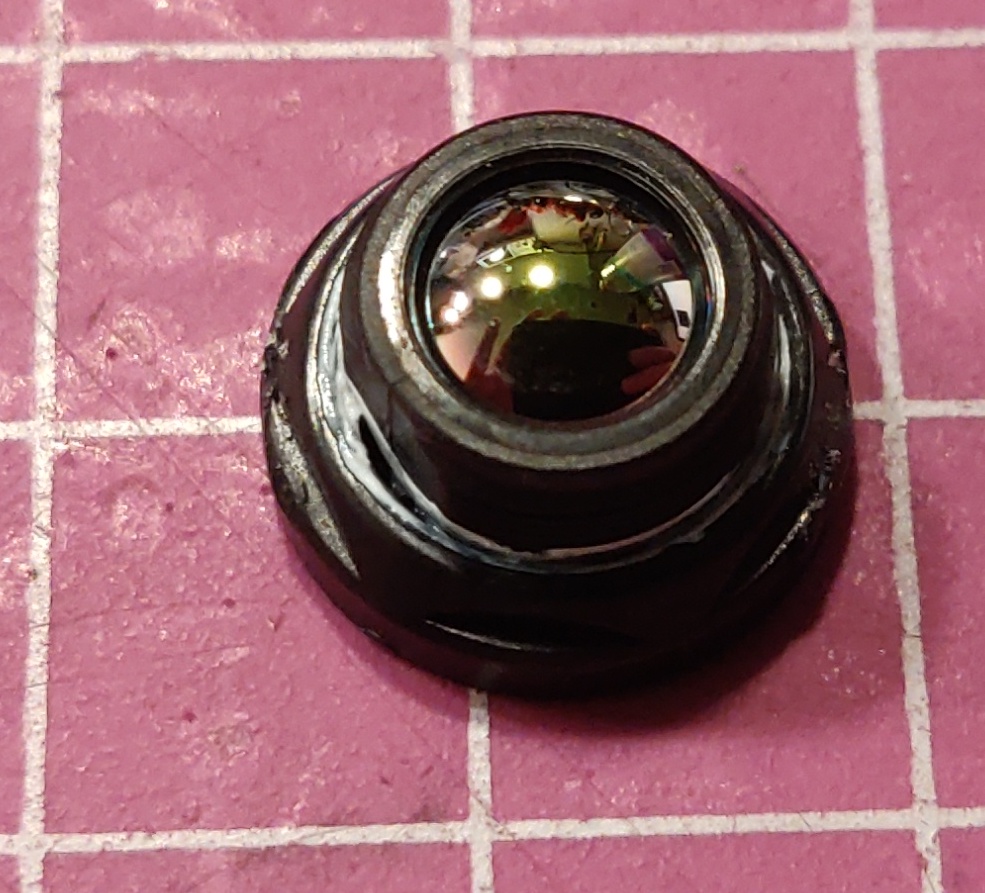
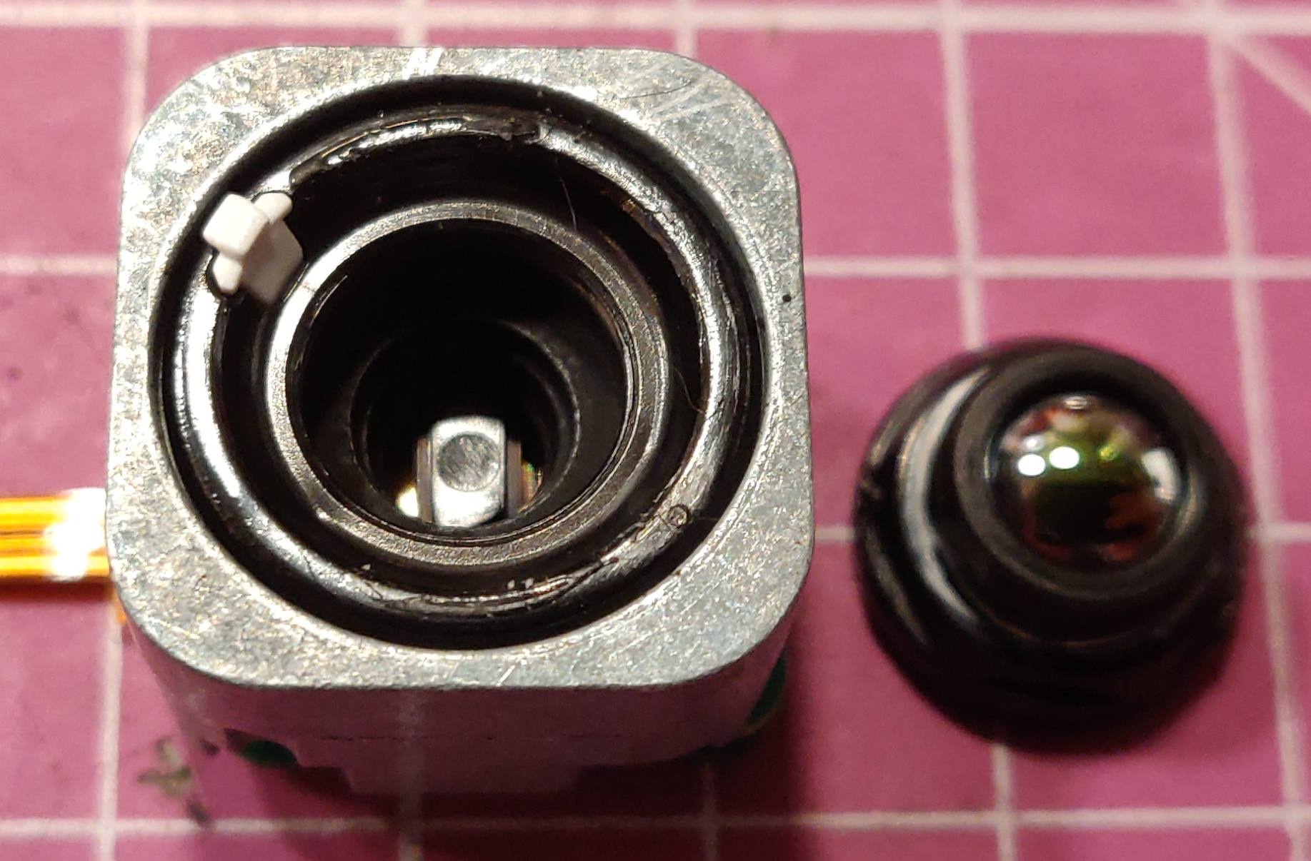
Front of the sensor has a removable lens, held in place with two daubs of what seemed to be hot-melt adhesive. It was easily removed with a scalpel. I am planning to design and 3D-print a tool that fits into the holes in the front to be able to set the focus.
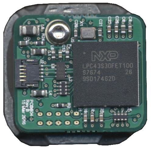
The processor on the thermal module is the NXP LPC4330FET100, a Dual-core Cortex M4/M0 chip. More info here
The camera module is a sandwich of two boards – front board holding the directly bonded sensor (this is pure speculations)
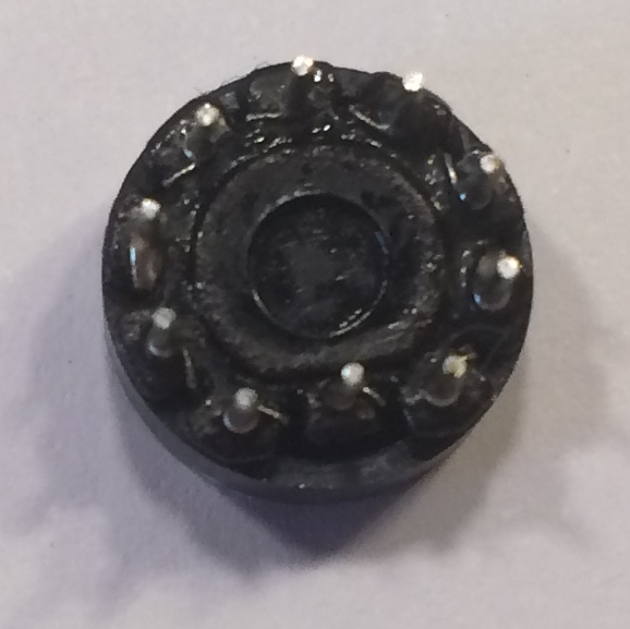
Bottom side of main PCB with the NXP micro holds some support circuitry and a big SPI flash that holds the firmware that runs the module.
On top of the main board, in vicinity of the thermal module there is U100, it’s a bog-standard DS18B20 thermometer for local compensation of the camera’s own temperature. I guess the thermal module does not carry its own temp. sensor.
Some playing around with booting the board without thermal imager or visible camera modules revealed that with both unplugged it will hang indefinitely at the boot screen (but it will still switch off when you press the power button, so it’s not dead behind the scenes). Unplugging only one of the cameras/sensors will have the camera booting happily. Unplugging the visible camera makes all mixed image modes go black. Unplugging the thermal module makes all thermal readings go away, but you can still use the visible module just fine. I guess it was built this way to not die completely if one of the devices went bad, but instead would boot and the user could see what was missing, to go report the error and get the device off for repair.
On the back of the board there is a switch, S1. I tried pressing it while the unit is in operation, no response.
Holding it down while pressing power button yields a device that does not boot, but rather “locks up” – I’m pretty sure this button is to go into some bootloader flash mode. The firmware talks about a “fel button” – it’s for firmware flashing as far as i know for now.
Well this is getting interesting!
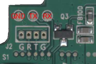
The small connector footprint J2 showed to contain no output at all, i scoped it and it’s dead as a dodo.
The three test pads over it on the other hand is alive and well with debug serial@115200 8N1 – YEAH!
Booting the camera with all devices connected will yield this nice bootlog:
HELLO! BOOT0 is starting!

boot0 version : 3.1.0

reg_addr 0x01f00100 =0x00000000

reg_addr 0x01f00104 =0x00000000

reg_addr 0x01f00108 =0x00000000

reg_addr 0x01f0010c =0x00000000

reg_addr 0x01f00110 =0x00000000

reg_addr 0x01f00114 =0x00000000

DRAM DRIVE INFO: V1.5

DRAM CLK =552 MHZ

DRAM simple test OK.

dram size =512

card boot number = 2

card no is 2

sdcard 2 line count 0

[mmc]: mmc driver ver 2014-07-07 16:54

[mmc]: ***Try SD card 2***

[mmc]: mmc 2 cmd 8 timeout, err 0x00000100

[mmc]: mmc 2 cmd 8 err 0x00000100

[mmc]: mmc 2 send if cond failed

[mmc]: mmc 2 cmd 55 timeout, err 0x00000100

[mmc]: mmc 2 cmd 55 err 0x00000100

[mmc]: mmc 2 send app cmd failed

[mmc]: ***Try MMC card 2***

[mmc]: MMC ver 4.5

[mmc]: SD/MMC Card: 4bit, capacity: 3728MB

[mmc]: vendor: Man 0x0090014a Snr 0x012084b9

[mmc]: product: H4G2a

[mmc]: revision: 1.1

[mmc]: ***SD/MMC 2 init OK!!!***

sdcard 2 init ok

The size of uboot is 0x000bc000.

sum=0x0ccccd69

src_sum=0x0ccccd69

set_mmc_para,sdly 50M 0

set_mmc_para,sdly 25M 0

Succeed in loading uboot from sdmmc flash.

Ready to disable icache.

Jump to secend Boot.

[      0.335]
The rest is not shown here, open BOOT down here under to see the full bootlog.
Raw logs from boot can be found here – some of them is booting without imagers connected, just to see how it reacts:
System is running Busybox, and with some serial debug magic i managed to copy files from system folders to the /mnt/IMGS folder that is exposed over USB. I found all kind of good stuff there – in /boot/ i found logos for other manufacturers (different branding), the cheesy battery recharge-animation – even audio files though the system has no way of doing audio recording or playback 😀